ISI is leveraging our deep experience with IC obsolescence solutions to solve our customers’ component supply problems with customized interposers to match their existing PCB footprint. Watch this webinar to learn how ISI can help your organization circumvent supply shortages through the development of IC adapters and interposers. ISI can design and manufacture a replacement device to emulate your original IC and fit an existing PCB footprint. Our alternative solutions help to keep your production line up and running while avoiding costly board re-spins and gray market buys.
This webinar is designed to educate the audience about the different types of adapters we can produce to replace unavailable or outdated ICs. Our expert panelists provide real-world examples and an overview of our collaborative process for developing and manufacturing footprint conversion adapters for various applications. The presentation is followed by a question and answer session with our panelists.
Hello and welcome to today’s webinar, Adapt to the Component Supply Crisis: Alternative Solutions for the Semiconductor Shortage.
Today’s webinar will have two presenters that will be followed by live Q&A.
First, Tom Casey will discuss how the supply chain shortage is affecting ISI’s customers. He’ll provide a brief overview of our design and manufacturing capabilities to develop interposers and adapters for a wide range of applications.
Next, we’ll hear from John Moore, ISI senior electrical engineer. John will dive right in to explain the different types of adapter designs that we can produce from very simple to highly complex using real-world examples. He’ll also provide a clear overview of our collaborative design process along with estimated timelines for our interposer project development.
Now, I’ll hand the presentation over to Tom Casey to get started.
Tom Casey, VP Inside Sales, ISI
Thanks for that introduction, Peter. First, let me provide you a little bit of information on ISI.
ISI has been manufacturing interposers and advanced packaging modules for over 30 years. In 2016, ISI was acquired by Molex and became part of the Molex Datacom and Specialty Solutions division. Today, ISI designs and manufactures a variety of interposers, electronic assemblies, and connectors for customers across the globe in several different industries and for a variety of different applications.
We are located in Camarillo, California in Ventura County, about 1 hour north of the city of Los Angeles.
In today’s webinar, we want to talk to you about an exciting solution that ISI can provide to help our customers address the supply chain shortages which are so common in today’s electronics industry.
Supply Chain Shortages Abound
Shortages, long lead times, line down, expedite fees, high-cost brokers. All these phrases are familiar to us here in the electronics industry.
There’s a supply chain shortage for vital semiconductor products. These shortages are preventing customers from shipping their products. Customers’ inability to ship products is impacting their financial performance and preventing them from meeting their revenue and profit objectives.
Customers are faced with the choice of waiting for these components or utilizing non-traditional suppliers which can be risky and costly. Another option—redesigning their boards—can trigger re-qualifications or time-consuming regulatory recertifications.
ISI Can Provide an Alternative
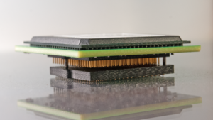
ISI can provide an alternative to these long lead time components. ISI can design and manufacture replacement devices. And these replacement devices generally are comprised of a new component which is available, a printed circuit board, and a mechanical attachment scheme to mimic the original device footprint.
These replacement devices can fit the existing PCB footprint and when designed properly can function in the customer’s system. Our replacement devices allow customers to avoid those costly redesigns, re-qualifications, and recertifications from regulatory bodies.
ISI’s Collaborative Engagement
The solution ISI provides is designed through a collaborative engagement with our customer. ISI’s engineering team will collaborate with the customer’s engineering team to design a replacement device that can be integrated into the customer’s product.
ISI engineers will collect information for the design such as:
ISI Makes Different Types of Adapters
ISI can make replacement devices for all types of different devices. Just really whatever the footprint is of the original device that you cannot get, whether it be a BGA adapter, a leadframe adapter, PGA/DIP/SIP — we can make it. If it’s an industry standard, we typically have made it before, and if your replacement device has a unique footprint, we usually can figure out a replacement for that as well.
Why choose ISI for these interposers? Well, there’s two reasons.
Engineering Advantage
Number one, our engineering advantage. ISI’s engineering has been designing these interposers and IC obsolescent replacement modules for over 30 years. ISI’s engineering team has system-level expertise with deep knowledge of FPGA devices. So, we can interact with your system-level people to make sure the device is designed properly.
We have an in-house PCB design team with deep experience utilizing DFM (design for manufacturing) approach to lay out a variety of different types of boards to be manufactured with a high degree of quality.
Our in-house test development goes from a simple JTAG test to full functionality, and our engineers who develop these tests are located right here in Camarillo near our production line. So, we can quickly prototype and then bring a product to production seamlessly for our customers.
Manufacturing Advantage
The second reason is ISI has a manufacturing advantage.
We’ve been manufacturing these interposers for over 30 years right here in Camarillo. We have an experienced SMT manufacturing team that utilizes innovative manufacturing techniques to ensure quality in production.
We have vast re-balling experience and capabilities which we leverage for our BGA interposers and modules.
ISI designs and assembles our test boards right here in Camarillo as well. So, there’s tight linkage between our design test engineers and the operations team to bring the testing online quickly and ramp to production.
Now I’d like to introduce you to our chief design engineer, John Moore. John will go into a bit more technical detail on the things we consider when designing replacement interposers. John?
John Moore, Senior Electrical Engineer, ISI
Thanks Tom. Again, I’m John Moore and I’m a senior design engineer at ISI with extensive experience in designing digital boards to customer specifications.
Today, I’d like to focus on adapters for FPGAs.
Footprint Conversion Adapters
FPGA adapters can range in complexity from simple to more complex depending on the differences between the original part and the replacement part.
The simplest adapter would have a replacement part no larger than the original part with no power or IO voltage differences.
The first adapter shown on the left is an example of such a design.
When the replacement part requires different power supply voltages and these cannot be provided by the motherboard, or possibly IO levels that are incompatible with the replacement part such as a lack of 5V tolerance, then extra circuitry is required on the adapter such as LDOs or level converters.
The middle example had those requirements. In this example, the replacement part was much smaller than the original, leaving room for the level converters for the IO and for the LDO for the power supplies.
The best scenario in an adapter design is if all the parts that are required to replace the original fit within the footprint of the original part.
That’s not always the case.
In the case of the third adapter shown, the replacement part was the same size as the original and yet it did require different power supply voltages to be provided by the adapter.
In these cases, we would collaborate closely with the customer, sharing DXF files and the like, to find a way to expand the footprint of the adapter without interfering with components on the board that it mounts to.
Now this added complexity will increase the design time and thus the NRE cost and very likely the repeat cost of the unit, but it is possible.
As Tom mentioned, we can accommodate many types of connection methods to match the original footprint.
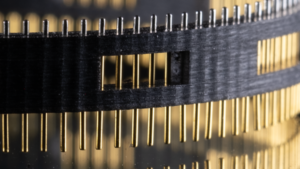
I think the most common seems to be BGA.
For BGA devices, the balls—may not be obvious—but the balls are attached during assembly so that the end result is an adapter that can be placed on the original footprint by your contract manufacturer with no special handling.
Overview of Adapter Design Process
Next, I’ll go through the typical process for designing an adapter.
Now, the process, as you might guess, starts by talking with the customer to understand the requirements.
We do have a standard questionnaire that answers the most common questions such as the ones listed there:
If there are no showstoppers in the questionnaire answers, then we would write up a quotation for that adapter.
The quote will contain a breakdown of NRE costs and also provide a per-piece price for both the initial prototypes (which should be higher because the volume is going to be much smaller) and also a higher quantity production piece price.
The NRE will also cover the design and assembly of a custom JTAG fixture. I’ll be talking more about the JTAG fixture in the next slide.
Once a purchase order is received, then we can start the design process.
We generally hold a design review once the adapter PCB is completely routed. So, there’s a gate between start of design and fabrication.
We can also provide a 3D model such as a STEP file that the customer can use to model the adapter on their board.
After the customer signs off on the design, then we order the adapter PCB and all other parts, if there are, to make up the adapter.
For the replacement parts, it’s fairly common for that to be purchased by the customer and what we call “consigned” to ISI rather than ISI going and procuring the part.
After assembly and test of the adapter, we package the initial prototypes and send the units to the customer for evaluation and testing.
In some cases, that validation can take a fair amount of time and could include shock and vibration or any number of environmental tests. So, there might be quite a time gap between initial prototype delivery and a follow-on order.
Once the design is validated, then the customer places a volume order.
Timeline for Adapter Development
Okay, here’s a flow chart showing the typical timeline for a new adapter design.
So, we start with a customer input, which would including the questionnaire I mentioned. This leads to a feasibility study ending with creation of a quote back to the customer for that particular adapter. This process typically takes 1 to 2 weeks.
The customer then places a purchase order that includes the NRE plus the initial prototype units. Again, these will be more expensive per piece than production quantity owing to the smaller volume.
During the design process, it’s common to collaborate with the customer on things like I/O assignments. While we might start with a suggested list of assignments, during PCB design it’s typical to recommend pin swaps that help simplify the rat’s nest on the PCB and possibly lead to fewer routing layers.
The PCB design process usually takes 2 to 4 weeks. If I/O swapping is recommended, we then get customer sign-off on the swapped I/O before actually proceeding with PCB routing.
Once the design is fully routed, we would hold a design review with the customer unless the adapter is so simple that no review is warranted. We can budget about one week for the review process, allowing for some back and forth for final tweaks.
After customer sign-off of the design, we order the PCBs and all parts used on the adapter. Again, the replacement part may be purchased and consigned by the customer.
Typically, PCB houses will quote between two and five weeks for the PCB. Any parts that were selected, let’s say for power supplies, would have been selected based on their availability, so they will fit inside that time frame.
Once all parts are received, we schedule a slot in our manufacturing line. It doesn’t actually take much time for the SMT process, but we need a window of time to set up and run the adapter through SMT and all the QA (quality assurance) checks. After assembly, the adapters are tested individually in a custom JTAG tester that verifies all connections and power supply levels if there were power supplies included in the adapter design.
The total time to assemble the adapters and test them usually takes between two and three weeks. The tested adapters are then packaged for shipment, usually on tape and reel or JEDEC trays which are, again, compatible with typical contract manufacturing processes.
So, the total time required from initial customer engagement to shipment of prototype adapters is usually between 8 and 14 weeks. Now for the production volume, the time required to buy all parts, assemble and test the adapters would be more like 4 to 8 weeks from receipt of order.
I hope this gives you a better idea of how long it takes for us to design and manufacture a custom adapter.
Interposer Manufacturing Process
Now adapters are, by their nature, small. So, they’re assembled on what’s called a multi-up PCB panel. Here you can see various kinds of interconnect we can use. On the next slide I’ll describe the manufacturing flow in a bit more detail.
The multi-up PCB panel is what we receive from the PCB house. The bottom side being the connection side is processed first. For BGAs that means attaching solder balls to all sides that have been screened with a solder paste stencil. Then the top side is screened with solder paste and all the parts for the top side are placed using state-of-the-art pick and place equipment. Then we reflow the entire panel in a Heller multi-stage IR reflow oven.
Finally, the adapters are singulated using a saw or router, whatever the design requires. Each adapter is visually inspected. We have automated optical inspection equipment (often called AOI) to detect defects and we can also measure parts for coplanarity etc. After QA checks, the parts are then tested again using a custom JTAG tester using a socket that matches the adapter’s footprint. We can also use a customer-supplied tester if that’s required. Then we package the parts using standard tape and reel, JEDEC trays, etc., or sometimes a custom-designed packaging if warranted or required.
An important part of the manufacturing process is verifying all connections from the adapter’s connector—in other words, the BGA or TQFP…in other words, the footprint of the original part—to the replacement part’s IO. We use industry-standard JTAG testing for this and design a custom tester for each adapter design.
Now beyond JTAG testing, there are optional testing available or we can perform that might include functional testing of some kind, thermal cycling. The design of the board allows for an environment other than room temperature. And we could also perform post-JTAG testing programming with the customer’s image, again, if that’s required.
Well, thanks for listening. I hope I’ve covered the process in a clear way and I’ve answered most of your questions. We will have a Q&A session here at the end in case something wasn’t covered. So, I’ll hand the presentation back over to Peter.
Thank you, John. And thank you, Tom. This concludes our main presentation on IC adapters and interposers as a viable option to replace unavailable components. Hopefully, this has been an informative session and we look forward to working with those of you who need such services.
And with that, let’s get started with the Q&A session.
Our first question is probably best suited for John, “How can ISI ensure that the TCE of the adapter will match the TCE of the board it mounts to?”
John:
Peter, that’s a good question and often asked by customers. There is concern that you’re introducing a variable that you didn’t have on your original board. Instead of mounting the unavailable IC, now you’re mounting essentially a little PC board with a replacement part.
In general, the motherboard—I refer to them as motherboards—the board that you’re going to solder this adapter down to—it’s going to be organic, it’s going to be FR4. There is some variation in TCE with various dielectrics perhaps, but in general that TCE is within a pretty tight range. And don’t forget you’ve got the solder of course—the solder interface from the adapter down to the motherboard for some compliancy.
So, it’s generally not an issue but it is something we can discuss with the customer specifically, oftentimes the customer’s reliability or manufacturing experts. So, if there’s any concern about TCE—thermal coefficient of expansion—we can discuss that, but in general it hasn’t been a problem.
Now, if it’s a ceramic board, that’s a whole different thing, but most organic materials we don’t have issues with, but it’s something we can discuss with the customer, okay?
Peter:
Very good.
I have another one that asks, “How can I make sure the interposer doesn’t reflow when I attach it on my board?”
John:
Yeah, I’m glad that was asked, again a common question. The truth of the matter is (depending on reflow profiles—but generally speaking) it’s going to reflow. Now that scares some folks, but let me step through it.
Let’s assume everything’s RoHS, right? The motherboard’s RoHS, and we don’t do anything special on the adapter. Everything’s RoHS. It’s going to have the same reflow profile. It’s going to have the same liquidus point, right? So okay, it reflows.
What happens? Well, we’ve had this discussion with several customers and oftentimes with our process expert in the loop, and the answer is even if it’s on the backside (in other words the second reflow and it’s facing down), generally speaking there’s enough adherence just from the solder that nothing falls off, right? There’s no movement and there’s no issues that would cause a concern.
However, it is common—I believe it’s standard practice for us—to what we call “tack down” or “corner bond” let’s say an FPGA that’s, I don’t know, 15, 20, 25 millimeters on a side, in other words, fairly sizable. We can epoxy the corners, ensuring that it doesn’t move and it won’t come off. That’s really just a belt and suspenders approach.
Again, our process engineer says, “No, no, I do this for a living. These things don’t fall off or move.” But we go ahead and offer that and like I said, I believe it’s standard practice to include that in our assembly process. So again, we can discuss it, but it’s generally not a concern.
Peter:
Sounds good, thank you.
Looks like I’ve got two questions that I’ll combine for Tom, “What is your minimum order quantity? Can you give a couple of examples of prices and volumes?”
Tom:
Sure, Peter. Thanks for that question.
So, we don’t typically have an MOQ per se. It’s really kind of a business case. Most of these efforts are customers who need to find a replacement device for thousands of parts which…as opposed to, like, 50 to 100 or something to that effect.
If it’s 50 to 100 pieces that’s not usually…there’s the same amount of engineering work to design an interposer for 50 to 100 pieces as it is for a thousand.
So, I would say, generally speaking, we’re working in the thousand-up range, but we have considered lower quantities.
And then as far as pricing goes, that can vary wildly depending on what the original device is. If it’s a simple integrated circuit device, then we’ve seen interposers that are, in high volume, as inexpensive as $15.
And then for more complicated, say an FPGA interposer, those can be north of $150 in high volume. So, it really…there’s a high range depending on the complexity of the design and the original component that you’re replacing.
And then the other factor is whether the customer is consigning the component to us or we have to go out and buy it. So, there’s a few things that can dictate the price. Hope that answers the question.
Peter:
All right thanks, Tom. Well, it looks like we’ve got through all of your questions and this concludes our webinar.
I’d like to thank everybody for watching and I hope that you found value in today’s presentation. I’d like to mention that all attendees will receive an email with a link to the webinar recording. If you have a need for IC footprint adapters, we encourage you to contact us to discuss your project. Thanks so much and have a great rest of your day.
Working with the ISI team is a highly collaborative engagement. The initial requirements customers bring are the starting point, but the big benefit comes as our engineers work to propose various solutions, including pros and cons of each. Those solutions include what many competitors can’t offer, which is in-house execution of nearly all aspects of the project.
Exchange technical details with customer to define challenges and establish scope of the project.
Assess likelihood of achieving the desired outcome and estimate the required engineering effort.
A quote will be issued to include NRE charges, price for prototypes and production volumes, and timeline for completion.
Design work begins with a particular focus on manufacturability. Frequent technical exchanges with the customer ensure a design that meets their expectations.
Upon customer approval, ISI initiates orders with suppliers and starts developing tools, molds, fixtures, and other custom equipment as required.
After satisfactory prototype testing and customer approval, product is released for volume production.
Your message will go to our in-house technical sales team. We typically get back within one business day.