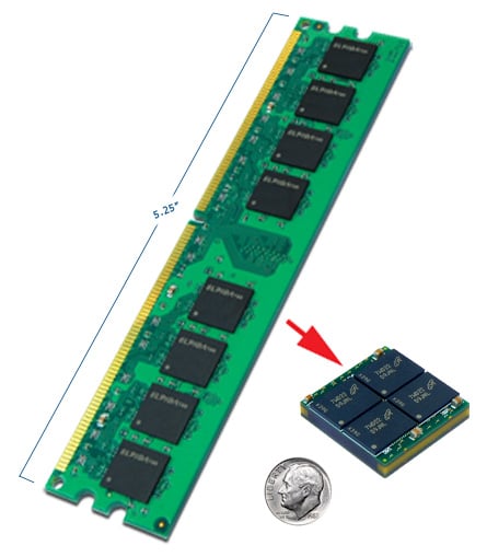
Specialized in Designing Miniaturized Electronics
ISI has been designing and manufacturing miniaturized electronics solutions for over three decades. Experience tells us that the key to a high-quality, reliable microelectronics solution is a well-thought-out PCB design. Our PCB designers are committed and follow a strict product development process that has enabled ISI to consistently deliver high-reliability solutions to a wide range of industries, such as Aerospace & Defense, Industrial, Medical and Transportation. Outlined below are the essential elements of our Design and Development disciplines that distinguish ISI from design firms, PCB fabricators, and contract manufacturers.
Requirement Capture
ISI’s broad experience in a variety of industries coupled with our highly skilled engineering team allows us to collaborate with our customers to quickly capture the critical requirements such as desired size, weight, and power (“SWaP”) for their specific application.
These technical exchanges foster a collaborative relationship with our customers, so they view ISI engineering as a natural extension of their own engineering team. Together, the teams further define and capture key electrical, mechanical, thermal, environmental and reliability requirements to develop a more comprehensive product specification. ISI’s engineers will also recommend design improvements to improve the manufacturability, quality and cost of the overall design. Once a specification is agreed upon, the design effort is initiated.
PCB/Substrate Design and Layout
ISI’s PCB design team utilizes state of the art design tools, industry standard practices, and internally developed design guidelines and specifications. ISI’s extensive engineering experience and flexibility allow us to intercept a project at various stages:
- CONCEPT
Customer’s design input requirements are thoroughly reviewed and evaluated. A design kick-off initiates a line of communication with the customer and the ISI project team. This relationship establishes tight technical exchanges and gains alignment on the project’s goals and timeline.
- SCHEMATIC DESIGN
During schematic generation, ISI’s project lead designer works closely with the ISI’s electrical engineer(s) and the customer. The schematic is reviewed and evaluated internally, then provided to the customer for feedback and approval.
- PRELIMINARY LAYOUT AND MANUFACTURABILITY
With the schematic, or connection list, and parts list provided by the customer, the board’s mechanical requirements are implemented. During this stage, ISI’s project lead designer engages with ISI’s procurement and mechanical engineering team on component selection and placement. Suggested changes and alternate components are presented to the customer at this time.
Before the PCB is routed, ISI’s project lead designer works with the board fabricator to ensure the board’s manufacturability and reliability. The board stack up (material selection, layer count and via structure) is typically established by the board fabricator and ISI at this stage. ISI’s PCB designers and manufacturing engineers have an internal review of the board design for manufacturability (DFM). The preliminary layout is provided to the customer for feedback and approval. The preliminary layout work, the extensive design reviews for manufacturability and ISI designer’s meticulous approach are the foundation for producing a high-quality design and a highly reliable end product.
- FINAL LAYOUT
The PCB is now ready for routing using relevant design rules. Once routing is complete, a design rule check and clean-up are implemented. Design review and verification are then completed. Assembly drawings, bill of materials and the PCB output files are generated for the Design Approval package. The Approval Package is also evaluated internally by another designer for verification. In additional, a cross-functional review is completed by Design Engineering, Manufacturing, Quality Assurance and Sales before Approval Package is sent to the customer for review and approval.
- FABRICATION
Once the customer signs off and approves the final design package, the documents are reviewed once more and signed off by each department manager/lead at ISI. When all documents are signed off, the final data is placed on order with the PCB fabricator. The fabricator reviews and preps the step & repeat data for fabrication. The ISI PCB designer works closely with the fabricator to answer Engineering/Technical Questions. The final fabrication artwork is reviewed and approved by the ISI PCB designer at which point the fabricator proceeds with PCB production.
Partner with ISI to Achieve Smaller Modular Solutions
Our proven collaborative design process is what distinguishes ISI from its competitors. A high-quality printed circuit board is the lynchpin to a high-reliability microelectronic solution and the reason customers continue to choose ISI as both their design and manufacturing partner.